Press releases
Reliable and faster chip designs through invasive and parametric simulation methods
Dissertation on new methods for automation in integrated circuit design
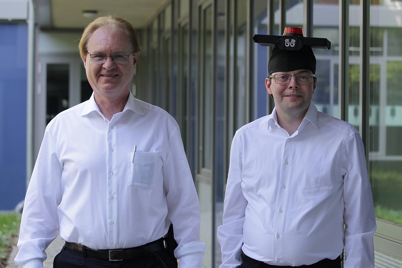
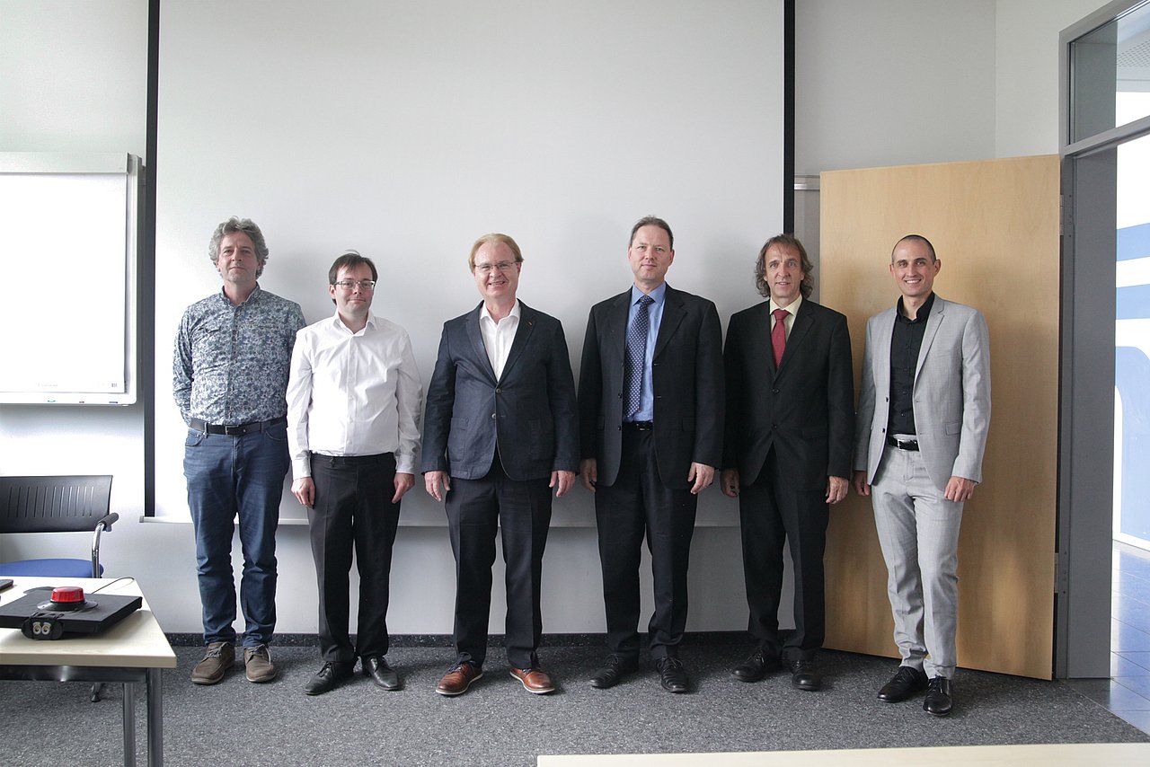
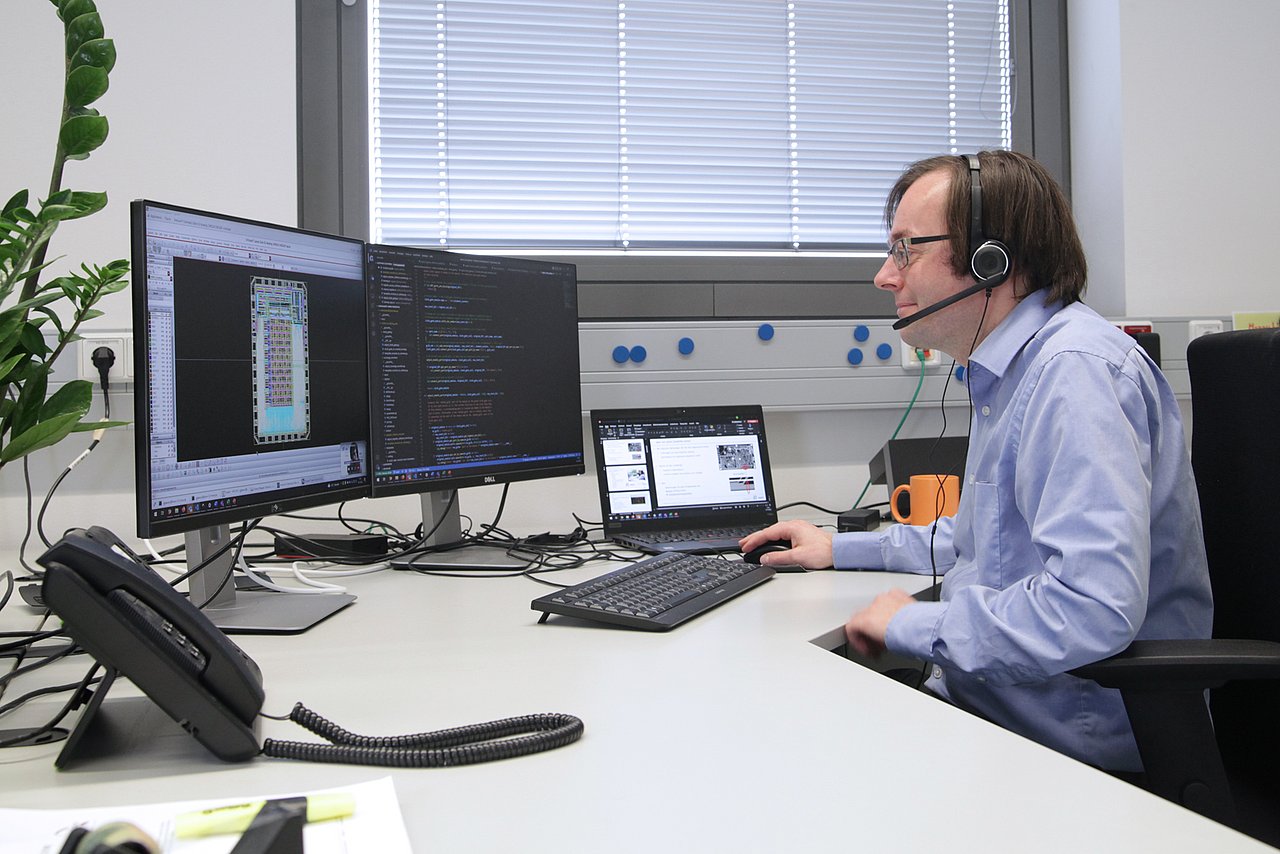
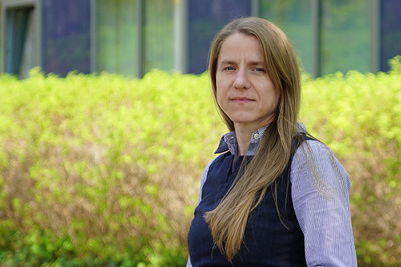
Ilmenau, 15 June 2023: Georg Gläser, specialist for the integration of AI methods in design automation at IMMS, successfully defended his dissertation “Invasive and Parametric Simulation Methods for Integrated Circuit Analysis” in Ilmenau on 14 June 2023. His work, which was created at IMMS, addresses the fundamental problem in the design of analogue and mixed analogue-digital integrated circuits: These chips, which are part of every smartphone or enable IoT applications, are partly designed manually -despite Electronic Design Automation (EDA) - and then simulated. Causes of errors are searched for and eliminated on the basis of experience before the expensive and time-consuming semiconductor production starts. The aim of Georg Gläser's methods is to support this error search with innovative EDA methods. The main idea of his work is to use automated model refinements for the development of integrated circuits to include and understand problematic effects. This is achieved through targeted changes in parameters and structures, which can be used to find previously unknown information about an integrated circuit, combine it and use it to improve the circuit design. All methods were tested in chip developments at IMMS. The results are used and followed up in various research and industry-driven chip design projects and are the basis for the AI-based design and test automation researched at IMMS.
Simulation and verification of analogue and analogue-digital integrated circuits shaped by empirical knowledge
“In chip design, problems often come to light very late - for example, during the layout, which is the construction plan that is developed for production in the end. Then, in extreme cases, you suddenly realise that, for example, lines are too close together and can impair performance through crosstalk or even destroy a chip in interaction with other effects,” explains Georg Gläser. It takes a lot of time to go through the causes of errors from the individual transistor, of which there can be millions in a circuit, to the complex overall system design level by design level, because all these levels have to be described in detail with models and simulated, Georg Gläser continues. “The main problem, however, is that the models have not been able to show many effects so far. This is because people often work with simplified macro models that usually do not represent noise, parasitic couplings or unfavourable effects of deeper design levels.” So far, only experience has helped. Moreover, existing methods usually start at only one design level. In addition, the systems and hence the necessary simulations are becoming more and more complex, as more and more functionality and thus circuit elements are to be put on ever smaller chip areas.
Methods provide more knowledge about the circuit and reduce design costs
On the one hand, the methods make it possible to integrate interference effects into the models to map them in more complex simulation scenarios. On the other hand, the methods provide insights into areas in which the models, circuits and systems work and where they do not. In addition, the methods make it possible to estimate design uncertainties at an early stage and to reduce iterations in the design and thereby decrease costs. For example, one method, the symmetry search for parasitic elements, delivered 223 possible problem areas as a result for a contact image sensor chip development at IMMS after only 6 hours of computing time, which would otherwise have had to be found by hand. Another method for identifying problematic couplings in the layout was already successfully used by industrial partners of IMMS before the dissertation was published.
The dissertation presents five methods that can be used at each design level or at the transition to the next. This is a clear advantage compared to other contributions, which are usually limited to one level in the design process. Some of the new methods are described here as examples.
Invasive analysis for early detection of previously unconsidered effects
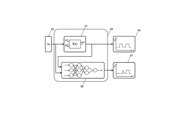
Using an invasive analysis, system models can be dynamically adapted in the work to gain insights into possible or existing disturbing influences, such as coupling of lines. The framework developed for this with several 10,000 lines of code is suitable for very complex systems and can analyse the programme code of behavioural models, adapt the models accordingly and address the simulator. For example, parasitic elements are inserted or removed in this way, or test and observation modules are added.
Parasitic symmetry analysis and acceptance regions
Many problems are often only visible in the layout, e.g. when couplings occur due to closely spaced lines and thus enable signal paths that result in undesired effects. Up to now, troubleshooting after the layout is done by trial and error with many manual simulations to find out where the error comes from, sometimes also with statistical methods. A systematic approach for the analysis of mixed-signal systems before layout was missing.
The starting point of the new approach of symmetry analysis is that symmetry is a core concept in circuit design itself. The idea behind this is to find interfering operating conditions that are symmetrical, therefore neutralise each other and can thus be eliminated from further troubleshooting, similar to headphones with Active Noise Cancelling, which can cancel out noise with exactly opposite signals of the same strength so that they are no longer perceived as annoying.
To be able to map and analyse these interference variables, which are not present in the circuit diagram, the method of acceptance regions is used. With it, symmetries can be made visible and derived as a basis for the search algorithm. Behind this are complex algorithms that examine all possible symmetry pairs with maximum values. The method classifies the parameter space into segments that show where the system works and where it does not. The advantage of the method is that the layout does not have to be known.
Basis for research into AI-based design and test automation at IMMS
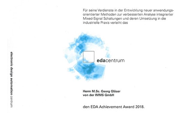
When Georg Gläser was honoured with the EDA Achievement Award by the edacentrum long before he submitted his dissertation, it was already confirmed that his work is an important contribution on the way to further design automation of analogue and mixed-signal circuits, opens up new optimisation potential in circuit design and significantly expands the state of the art in EDA. Prof. Dr.-Ing. Ralf Sommer fully shares this assessment. As Georg Gläser's doctoral supervisor, scientific director of IMMS and Head of the Department of Electronic Circuits and Systems at the Faculty of Electrical Engineering and Information Technology at Technische Universität Ilmenau, he adds: “With his methods, Georg Gläser has also set the course for research on AI-based design and test automation at IMMS, which he has decisively shaped and for which he has systematically built up a team of experts in recent years to further advance the topic.” Under his leadership, research groups and projects were also acquired and worked on to expand know-how in this area. On this basis, a range of services for the methodological support of industrial customers was established. In addition, he has initiated further dissertations in this field in his team, which are very promising, Sommer continues. “We are curious to see what the future entails. Georg Gläser has made a great contribution, of which we are very proud.”
This might also be interesting for you
Related content
Project
VE-VIDES
Against hacker attacks: Innovative chip architectures, modelling and verification methods for trustworthy electronics
Project
VE-ARiS
IMMS developed copy protection solutions for integrated circuits to secure the know-how of partners
Project
KI-EDA
IMMS developed smart models and tes methods for the design of sensor and control chips for I4.0 applications
Project
IntelligEnt
The IMMS researched assistance systems for chip designers: Machine Learning improves design and test methods for integrated analogue/mixed-signal…
Patent
DE 10 2016 119 927
Circuit arrangement for providing the charging energy for a level change on a signal bus, calibration method and signal transmission system

Patent
DE 10 2016 113 283
Method for determining a resistive deflection of a Wheatstone bridge in a high temperature environment
Event,
SMACD 2024
International Conference on Synthesis, Modeling, Analysis and Simulation Methods and Applications to Circuit Design (SMACD)
Event,
Days of trustworthy electronics 2024
Presentations of the results of the research projects of the funding guidelines for trustworthy electronics (ZEUS) and future-proof special processors…

Event,
edaWorkshop 2024
edaWorkshop24 and the European Nanoelectronics Applications, Design & Technology Conference (ADTC)
Contact
Contact
Dipl.-Hdl. Dipl.-Des. Beate Hövelmans
Head of Corporate Communications
beate.hoevelmans(at)imms.de+49 (0) 3677 874 93 13
Beate Hövelmans is responsible for the text and image editorial work on this website, for the social media presence of IMMS on LinkedIn and YouTube, the annual reports, for press and media relations with regional and specialist media and other communication formats. She provides texts, photographs and video material for your reporting on IMMS, arranges contacts for interviews and is the contact person for events.


