Test and characterisation
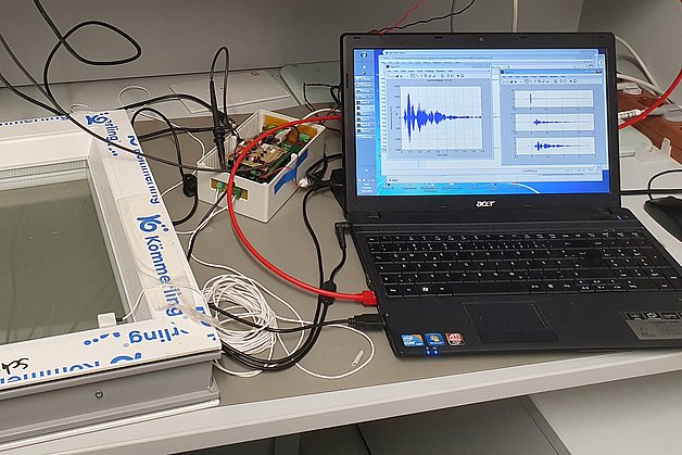
We test, characterise and qualify your circuits, sensors and systems. Based on our excellent pool of measurement equipment, we develop an individually adapted test environment for measurements on wafers and individual components. Our services range from measurements on transistors, circuits and assemblies to the characterisation of complex applications.
With our team we will support you with:
Together with you, we develop and optimise test setups to determine the parameters of your circuits and components accurately and quickly.
- Development of test methods
- Modular test platforms
- Development of application-specific test equipment
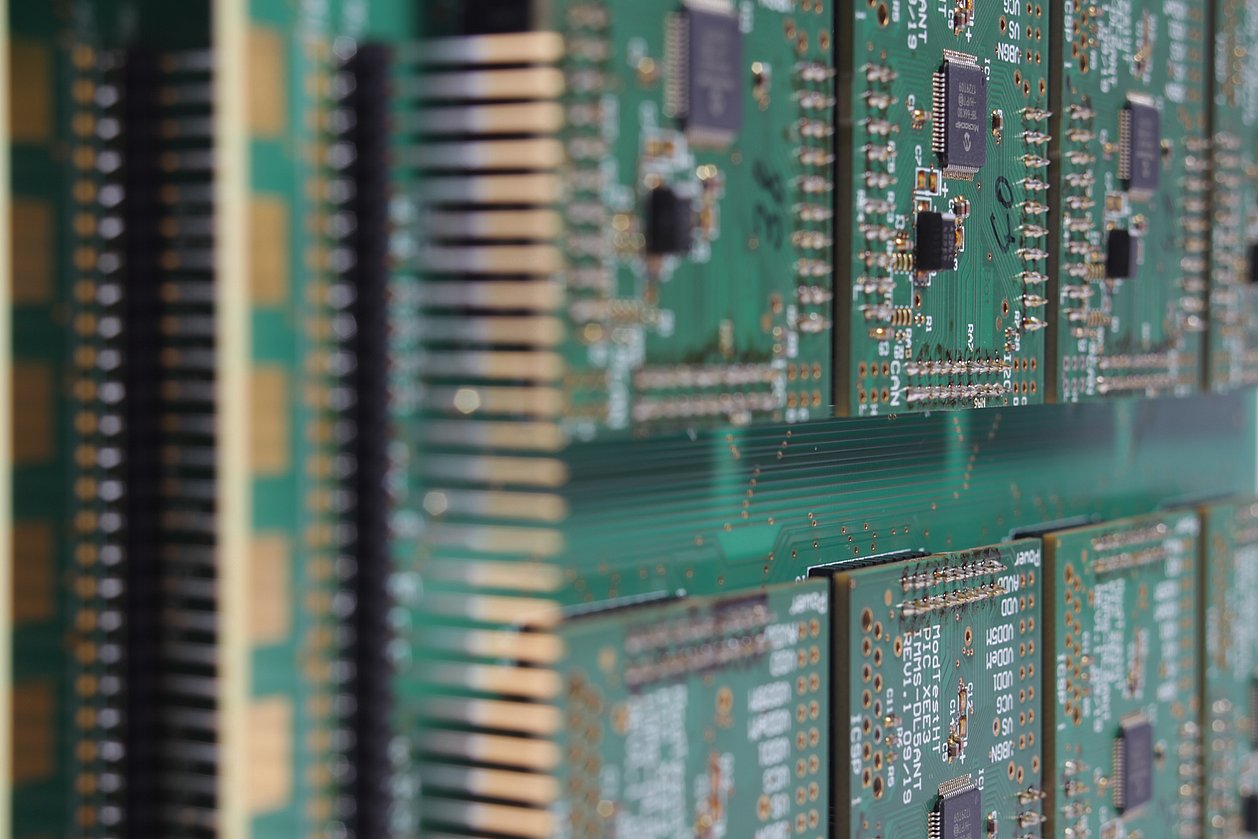
- Load board development for test platforms in production test
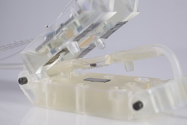
- Development of probe cards for wafer test
We support you in creating and optimising automatic test sequences to determine trustworthy and reproducible measurement data.
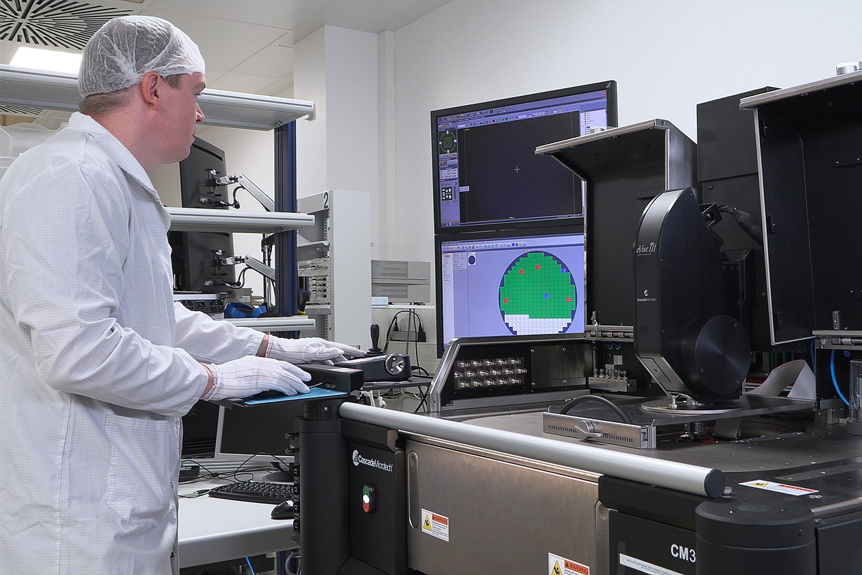
- Wafer test (max. 12'' wafer)
- PXI test systems
- Test programming (LabView, Python, C)
- Statistical measurement data evaluation
Thanks to our many years of experience in the development and implementation of small-series tests, we reliably ensure quality and adherence to schedules.
- Automated wafer test (max. 12'' wafer)
- Device test
- Test under temperature influence (-40 °C ... 300 °C)
- Quality assurance through statistical evaluation of measurement data
To predict the lifetime of your circuits and components, we work with you to develop an accelerated ageing setup and perform the necessary ageing tests.
- Development of setups for ageing
- Determination of stress conditions
- Evaluation of the ageing development
For the transfer of your developments into production, we organise qualification tests for components or packages according together with you.
- Planning and execution of qualification tests according to JEDEC standard
- Device qualification (HTOL, LTOL, Latch-Up, ESD, etc.)
- Package qualification (HTSL, UHAST, TC, etc.)
- Development of a suitable test environment
To ensure and monitor your high-quality technology and products, we offer development- and production-accompanying tests.
- Measurements of component parameters
- ESD investigations according to HBM and TLP standards
- Characterisation for semiconductor technology (CMOS, SOI, BiCMOS)
- Reliability and quality assurance studies for semiconductor manufacturers
For this, we use our many years of experience and expertise in the following fields:
- RF- and EMC-compliant circuit design and PCB layout
- Characterisation and test of ICs and assemblies (coaxial and on wafer)
- Impedance and S-parameter measurements up to 50 GHz
- Spectral and signal analysis up to 26 GHz
- Noise measurements up to 26 GHz
- Static and dynamic measurements on optical sensors
- Parameter determination on light sources
- Development of optoelectronic circuits
- Spectral investigations on light sources and detectors
- Measurement and application systems for single photon detectors (SPAD)
- Circuit design for power applications
- Static and dynamic measurements on power semiconductors
- Wafer test up to 1 kV
- Pre-compliance measurement of conducted emissions (EMC)
- Long-term tests on high-voltage components under the influence of temperature (HTRB measurements)
- HBM Standard
- TLP standard
- Wafer test
- Device test
- Test up to 300 °C
- Wafer test
- Device test
- Development of test solutions for high-temperature test
- Vibrometric measurements for the analysis of mechanical vibrations
- Electrical and capacitive vibration excitation
- Wafer test
- Device test
Contact
Contact
Dipl.-Ing. Michael Meister
Head of Industrial Electronics and Measurement Technology
michael.meister(at)imms.de+49 (0) 3677 874 93 20
Michael Meister is your contact for testing services, the development of test methodologies, and long-term measurements. He answers your questions on Modular and mobile test systems that we develop in our research in Smart distributed measurement and test systems as well as about testing and characterisation of integrated sensor systems. He is responsible for the test equipment at IMMS and will support you in the validation of ASIC and MEMS developments.
Related content

Project
RGBS
Development of a new retrofittable glass break sensor based on ultrasound technology with greater precision and robustness

Project
MikroGraph
IMMS is developing evaluation electronics for new, highly sensitive graphene sensor technology for on-site detection of micropollutants in wastewater.

Project
TSN test lab
In the Time Sensitive Networking (TSN) laboratory, IMMS is exploring the technological limits to the creation of data-intensive industrial real-time applications.

Project
MEMS-Vibro3D
Research infrastructure for the next MEMS generation: 3D vibrometer system and new broadband amplifier
Reference
Prof. Ronny Stolz and Dr. Theo Scholtes, Leibniz-Institut für Photonische Technologien e.V. (Leibniz-IPHT)
„IMMS implemented the functionalities we needed, such as a lock-in amplifier, a phase-locked feedback loop and an active laser frequency stabilisation as an FPGA design. We would very much like to continue the cooperation with IMMS in future joint projects.“
Reference
Alexander Zimmer, X-FAB Global Services GmbH, Erfurt
”IMMS was able to offer us valuable support due to its many years of experience in the field of measurement technology and circuit design for optical sensors. The reliable work and the trusting partnership is a highly valued basis for the cooperation with IMMS.”
Reference
Hans-Christian Fritsch, Ilmsens
“We were particularly pleased that we, as a start-up from Thüringen with IMMS as its research institute, were able to create an innovative high-tech solution with the Thuringian semiconductor manufacturer X-FAB. We appreciate the high level of expertise and flexibility as well as the customer-oriented and target-oriented way of working of the colleagues from IMMS.”
Reference
Christian Paintz, Melexis
“Particularly in the evaluation of measurement data, IMMS has impressively demonstrated that a learning algorithm is on a par with manual evaluation – while saving a great deal of time. We are also continuing to pursue methods for circuit and layout analysis, as we see great research and application potential here as well.”
Evaluierung und Test der Empfangsleistung von Funksystemen
Björn Bieske1. Michael Schenk2.38. ITG / GMM / GI -Workshop Testmethoden und Zuverlässigkeit von Schaltungen und Systemen (TuZ 2026), 22. - 24. Februar 2026, Potsdam, Germany
1IMMS Institut für Mikroelektronik- und Mechatronik-Systeme gemeinnützige GmbH (IMMS GmbH), Ehrenbergstraße 27, 98693 Ilmenau, Germany. 2Adolf Würth GmbH & Co. KG.HF-Messtechnik 2: Klein gegen Groß – nanoVNA: messen und kalibrieren
Björn Bieske1.HAM Radio, Internationale Amateurfunk-Ausstellung, Juni 27-29, 2025, Friedrichshafen, Germany
1IMMS Institut für Mikroelektronik- und Mechatronik-Systeme gemeinnützige GmbH (IMMS GmbH), Ehrenbergstraße 27, 98693 Ilmenau, Germany.Testsystem für die Charakerisierung analoger und digitaler Strukturen – Mixed-Signal-Analyse wird mobiltauglich
Tom Reinhold1.Elektronik, 24.2024, 26. November 2024, Seite 70 - 73, ePaper: wfm-publish.blaetterkatalog.de/frontend/mvc/catalog/by-name/ELE
1IMMS Institut für Mikroelektronik- und Mechatronik-Systeme gemeinnützige GmbH, Ehrenbergstraße 27, 98693 Ilmenau, Germany.Einstieg in die HF-(Mess-)Technik
Björn Bieske1.HAM Radio, Internationale Amateurfunk-Ausstellung, 28. - 30. Juni 2024, Friedrichshafen, Germany
1IMMS Institut für Mikroelektronik- und Mechatronik-Systeme gemeinnützige GmbH, Ehrenbergstraße 27, 98693 Ilmenau, Germany.


