Integrated Circuits
We offer the design and realisation of application-specific integrated circuits (ASICs) in CMOS, BiCMOS and SOI technologies. Many years of experience and profound ASIC development know-how are our foundation to find the best solutions for your application. Together with you we acquire a development concept leading to the perfected compromise between performance, operating conditions and manufacturing costs.
For the design of an integrated circuit we balance the limitations of accuracy and bandwidth, power consumption, chip size and the choice of technology as an example. Such a concept is then implemented according to our qualified ASIC design flow. Thanks to a close collaboration between our design and test engineers as well as with our manufacturing partners, we achieve well-performing ASICs with our first runs (first-time right silicon).
Our team consists of specialists for
- analog circuit design,
- digital circuit design,
- mixed-signal verification,
- opto electronics and
- radio frequency technology.
- Specification development,
- Circuit design and verification,
- Layout and test development,
- Wafer processing,
- Characterisation and test,
- Qualification and transition to manufacture.
We document all phases intensively and organize regular project reviews with our customers. We employ certified partnersfor all process steps that we cannot operate in-house, e.g. manufacturing and dicing of wafers, or wire bonding and packaging of the ASICs.
- Concept and feasibility studies
- System modeling and simulation
- FPGA and virtual prototyping
- Analog, digital and mixed-signal design
- Analog, digital and mixed-signal verification
- Layout design
- Synthesis and place-and-route
- Automatic Test Pattern Generation (ATPG)
- Precision amplifiers,
- radio-frequency (RF) circuit upto 5 GHz,
- high-voltage (HV) circuits upto 200 V,
- high-temperature (HT) circuits upto 300 °C,
- control loops,
- clocked circuits,
- integrated optical receivers,
- integrated sensors,
- digital interfaces,
- complex sequence controllers,
- embedded microcontrollers,
- firmware and driver software.
- Operational and instrumentation amplifiers (op-amp),
- transimpedance amplfiers (TIA) and charge-sensitive amplifiers (CSA),
- low-noise and power amplifiers (LNA, PA), mixers and filters,
- current and voltage regulators (LDO) and converters (DCDC),
- delta-sigma modulators (DSM) and phase-locked loops (PLL),
- bandgap, power-on-reset- (POR) and delay circuits,
- integrated photodiodes as well as temperature and pH sensors,
- self-test and calibration circuits (BIST),
- A/D converters (ADC) and D/A converters (DAC),
- communication interfaces (SPI, I2C, PWM, SENT, DALI),
- actor and bus drivers
- and other components.
We chose the appropriate design methodology
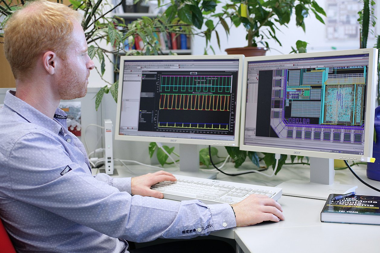
Being a Lead Institution for Analog Mixed-Signal Design Methodology in the Cadence Academic Network, we are familiar with the newest design methods and tools. For the implementation of a mixed-signal ASIC for instance, we use classical techniques based on Verilog-AMS as well as modern approaches for modelling and synthesis based on high abstraction levels with SystemC. Depending on the application, we always evaluate individually if your objectives are achievable with established or innovation practices.
We use the following design tools:
We are familiar with the latest Cadence design software. Our specially developed design environment software manages the design data as well as the setup of the design tools and controls the users’ access privileges.
Contact
Contact
Eric Schäfer, M. Sc.
Head of Microelectronics / Branch Office Erfurt
eric.schaefer(at)imms.de+49 (0) 361 663 25 35
Eric Schäfer and his team research Integrated sensor systems, especially CMOS-based biosensors, ULP sensor systems and AI-based design and test automation. The results are being incorporated into research on the lead applications Sensor systems for in-vitro diagnostics and RFID sensor technology. It will assist you with services for the development of Integrated circuits and with IC design methods.
Related content
Project
PANDIA
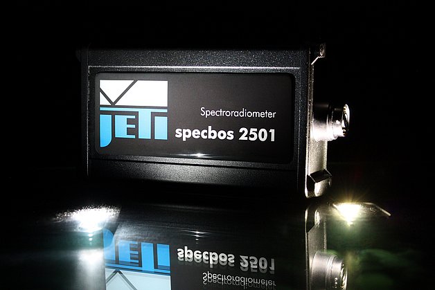
IMMS develops novel CMOS and SPAD sensor ICs for spectroradiometers for faster and more sensitive analysis of light
Project
SensInt
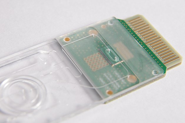
The IMMS is developing a CMOS image sensor for time-resolved fluorescence detection for direct integration into microfluidic cartridges using 3D screen printing.
Project
FluoResYst
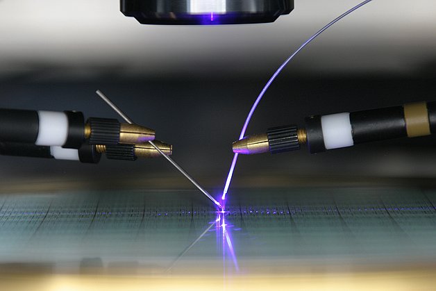
The IMMS is developing a SPAD-based sensor for time-resolved readout of fluorescence-labelled DNA microarrays.
Reference
Andrea Kulik, FRIZ Biochem
We were particularly impressed by IMMS’s ability to take a holistic approach to the interface between biochemical applications and electronic signal processing. This enabled our biochemical and technical requirements to be precisely translated into microelectronic concepts and implemented in a space-efficient manner.
Reference
Dr. Christof Steiner, DITABIS AG
IMMS can do much more than ‘just’ chip development – especially in the field of photonics and sensor technology. What we particularly liked: The IMMS team quickly and flexibly integrated itself into our network of DITABIS developers and external partners – with lots of ideas and a genuine team spirit.
CMOS-basierte Sensorsysteme für die In-vitro-Diagnostik
Alexander Hofmann1. Benjamin Saft1.elmug4future, Technologiekonferenz, Oktober 21-22, 2025, Jena, Thüringen
1IMMS Institut für Mikroelektronik- und Mechatronik-Systeme gemeinnützige GmbH (IMMS GmbH), Ehrenbergstraße 27, 98693 Ilmenau, Germany.Before It Hits the Chip: A Gentle Introduction to Mixed-Signal IC Verification
Martin Grabmann1.ISSOM 25, International Summer School on Microelectronics, August 25-29, 2025, Leibniz-Universität Hannover, Hannover, Germany
1IMMS Institut für Mikroelektronik- und Mechatronik-Systeme gemeinnützige GmbH (IMMS GmbH), Ehrenbergstraße 27, 98693 Ilmenau, Germany.Trust is Good, Monitoring is Better: FPGA- & TEE-Based Monitoring for Malware-Detection
Friederike Bruns1. Georg Gläser2. Florian Kögler2. Jonas Lienke2. Nithin R. Nanjundaswamy3. Gregor Nitsche3. Behnam R. Perjikolaei4. Jörg Walter4.13th IMA International Conference on Modelling in Industrial Maintenance and Reliability MIMAR2025, July 8-10, 2025, Université de Lorraine, France, DOI: doi.org/10.19124/ima.2025.01.25
1Carl von Ossietzky Universität Oldenburg, Oldenburg, Germany. 2IMMS Institut für Mikroelektronik- und Mechatronik-Systeme gemeinnützige GmbH (IMMS GmbH), Ehrenbergstraße 27, 98693 Ilmenau, Germany. 3DLR Institut für Systems Engineering, Oldenburg, Germany. 4OFFIS e.V. Institut für Informatik, Oldenburg, Germany.High-Sensitive Demodulator with Built-in Negative Offset Comparator for Passive UHF RFID Tags
Rohit Kesharwani1. Andre Jäger1. Martin Grabmann. Georg Gläser. Eric Schäfer1.IEEE RFID-TA 2024, Forum for advancing RFID technology and practice, Daytona Beach, FL, USA, December 18–20, 2024
1IMMS Institut für Mikroelektronik- und Mechatronik-Systeme gemeinnützige GmbH, Ehrenbergstraße 27, 98693 Ilmenau, Germany.


