Patent DE 10 2013 114 046
Electronic delay circuit in CMOS technology
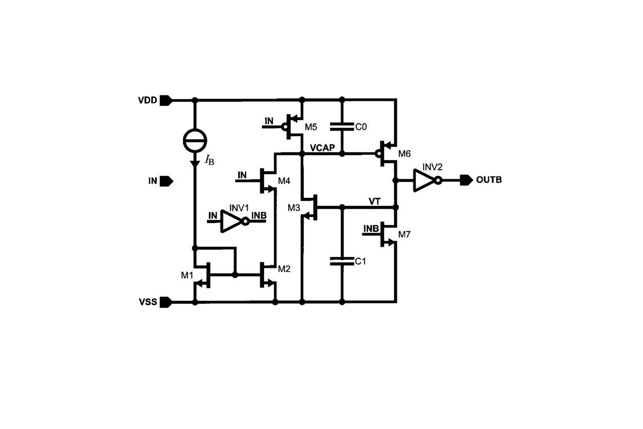
Electronic delay circuit in CMOS technology for emitting an output signal (OUT/OUTB) delayed in time with respect to an input signal (IN), comprising
- a CMOS thyristor primary switch formed from at least two transistors (M3, M6), whose switching signal (VT) occurring at the switching output is fed to a secondary switch which emits the output signal (OUT/OUTB);
- an integration capacitor (C0) which is connected between a supply voltage (VDD) and a node (VCAP) which connects the gate electrode of one transistor (M6) to the drain electrode of the other transistor (M3) of the primary switch and which can be discharged via a discharging means (M2);
- a switch (M4) which receives the input signal (IN) and is used to switch the discharging means (M2);
- reset elements (M5, M7) for resetting the primary switch (M3, M6) after the output signal has changed; characterised in that an additionally connected component is arranged at the switching output (VT) of the primary switch (M3, M6) as a discharge element (C1; M9) for discharging the sub-threshold current of the primary switch (M3, M6).
Patent No.:DE 10 2013 114 046
Inventor:Benjamin Saft. Eric Schäfer. André Jäger
Application:
Delay elements as a component of integrated circuits in energy self-sufficient systemsResearch field:Integrated sensor systems
granted patent
Application date:13 December 2013
Date of first publication:18 June 2015
Date of publication of grant:24 December 2015
Related content
Project
HoLoDEC
IMMS researches ultra-low-power architectures (ULP) and circuit concepts as well as energy-efficient edge-AI systems with overall system energy modeling

Project
StorAIge
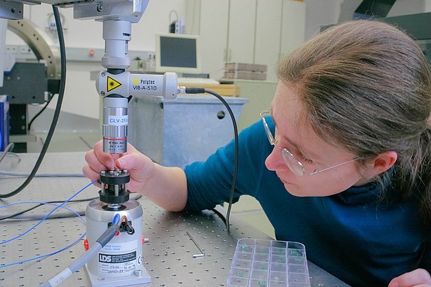
We are researching the use of ultra-low power embedded memories in wireless sensor front-end ICs for monitoring the condition of wind turbines and individual plants produced in greenhouses.
Project
GreenSense
For bio-analysis IMMS developed energy-efficient multi-parametric RFID microsensors and energy harvesting modules for operating autonomous sensors.
Press release,
Extended service life for self-teaching wireless sensors for industrial maintenance
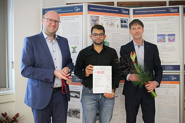
IMMS patent for edge AI solution wins bronze medal at iENA 2025
Press release,
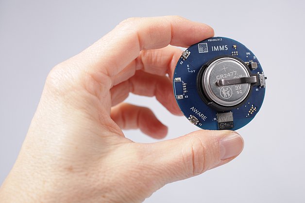
AI without the net: Energy-efficient edge AI sensor system for industrial monitoring applications
IMMS exhibits at embedded world
Press release,
Highly accurate and battery-free measurement via RFID
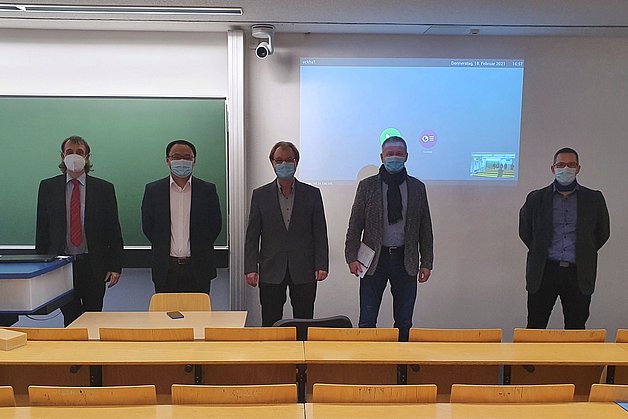
IMMS PhD candidate defends dissertation on precise passive RFID sensor technology
Case Study on Compression of Vibration Data for Distributed Wireless Condition Monitoring Systems.
Rick Pandey1. Felix Grimm2,3. Dominik Nille2. Christoph Böckenhoff2. Jonathan Gamez1. Sebastian Uziel1. Albert Dorneich2. Tino Hutschenreuther1. Silvia Krug1,4.Applied Sciences 2025, 15, 12346. DOI: doi.org/10.3390/app152212346
1IMMS Institut für Mikroelektronik- und Mechatronik-Systeme gemeinnützige GmbH (IMMS GmbH), Ehrenbergstraße 27, 98693 Ilmenau, Germany. 2Balluff GmbH, 73765 Neuhausen auf den Fildern, Germany. 3Institute of Smart Sensors (IIS), University of Stuttgart, 70569 Stuttgart, Germany. 4Department of Computer and Electrical Engineering, Mid Sweden University, Holmgatan 10, 851 70 Sundsvall, Sweden.Smartes Maschinenmonitoring – Anomalien mit Edge-KI detektieren
Sebastian Uziel1.in elektroniknet.de, 11. November 2025, www.elektroniknet.de/automation/industrie-40-iot/anomalien-mit-edge-ki-detektieren.228572.html und in Markt&Technik, Trend Guide Industrie 4.0/IIoT/KI 2025, S. 37-40, ePaper: wfm-publish.blaetterkatalog.de/frontend/mvc/catalog/by-name/MUT
1IMMS Institut für Mikroelektronik- und Mechatronik-Systeme gemeinnützige GmbH (IMMS GmbH), Ehrenbergstraße 27, 98693 Ilmenau, Germany.Application of the Expert Design Plan Methodology on an Ultra-Low-Power Sensor Frontend
Lorenz Renner1. Ralf Sommer1,2. Yannick Uhlmann3.2025 21th International Conference on Synthesis, Modeling, Analysis and Simulation Methods and Applications to Circuit Design (SMACD), July 7-10, 2025, Istanbul, Turkiye, pp. 1-4, DOI: doi.org/10.1109/SMACD65553.2025.11092185
1IMMS Institut für Mikroelektronik- und Mechatronik-Systeme gemeinnützige GmbH (IMMS GmbH), Ehrenbergstraße 27, 98693 Ilmenau, Germany. 2Technische Universität Ilmenau, Electrical Engineering and Information Technology, Electronic Circuits and Systems Group, Ilmenau, 98693, Germany. 3Electronics & Drives, Reutlingen University, Reutlingen, Germany.High-Sensitive Demodulator with Built-in Negative Offset Comparator for Passive UHF RFID Tags
Rohit Kesharwani1. Andre Jäger1. Martin Grabmann. Georg Gläser. Eric Schäfer1.IEEE RFID-TA 2024, Forum for advancing RFID technology and practice, Daytona Beach, FL, USA, December 18–20, 2024
1IMMS Institut für Mikroelektronik- und Mechatronik-Systeme gemeinnützige GmbH, Ehrenbergstraße 27, 98693 Ilmenau, Germany.

Event,
SMACD 2025
International Conference on Synthesis, Modeling, Analysis and Simulation Methods, and Applications to Circuit Design
Event,
InnoCON 2025
Innovation policy flagship event of the German Land of Thüringen. Topic “Key technologies: Paving the way for the world of tomorrow“
Contact
Contact
Eric Schäfer, M. Sc.
Head of Microelectronics / Branch Office Erfurt
eric.schaefer(at)imms.de+49 (0) 361 663 25 35
Eric Schäfer and his team research Integrated sensor systems, especially CMOS-based biosensors, ULP sensor systems and AI-based design and test automation. The results are being incorporated into research on the lead applications Sensor systems for in-vitro diagnostics and RFID sensor technology. It will assist you with services for the development of Integrated circuits and with IC design methods.
Contact
Dr.-Ing. Ludwig Herzog
Head of Mechatronics
ludwig.herzog(at)imms.de+49 (0) 3677 874 93 60
Dr. Ludwig Herzog will provide detail on our research on magnetic 6D direct drives with nm precision for the nm measurement and structuring of objects. He supports you with services for the development of mechatronic systems, for simulation, design and test of MEMS as well as for finite element modelling (FEM) and simulation.
Contact
Dr.-Ing. Tino Hutschenreuther
Head of System Design
tino.hutschenreuther(at)imms.de+49 (0) 3677 874 93 40
Dr. Tino Hutschenreuther will answer your questions on our research in Smart distributed measurement and test systems and the related core topics Analysis of distributed IoT systems, Embedded AI and Real-time data processing and communications, on the lead applications Adaptive edge AI systems for industrial application and IoT systems for cooperative environmental monitoring as well as on the range of services for the development of embedded systems.
Back


