Forum Künstliche Intelligenz
Use of Multi-Sensors in Predictive Maintenance – The Drill Tool Predictions using AI
Ist das Kunst? Machine-Learning-basierte PCB-Layoutanomalieerkennung in KiCAD mit AnoPCB (Is this art? Machine learning based PCB layout anomaly detection in KiCAD with AnoPCB)
Umut Onus
Georg Gläser
Abstract:
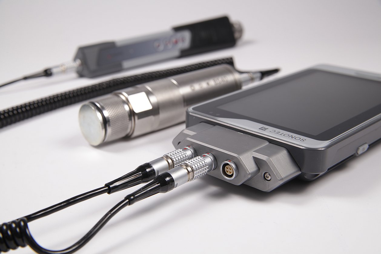
Use of Multi-Sensors in Predictive Maintenance – The Drill Tool Predictions using AI
Artificial Intelligence (AI) is enabling Predictive Maintenance (PdM) which is crucial to reduce unexpected production system downtimes and maintenance cost. Machine or tool condition estimation are the central tasks that should be performed on premise close to the machine, like traditional monitoring approaches. This requires that the relevant data is collected at the machine, processed there and AI models are deployed on embedded hardware perform the analysis. Several challenges arise to make this scenario reality as often the analysis stops at a well performing model on a server or the cloud.
First, there are numerous options to collect corresponding information, such as vibrations, acoustics emissions, force, temperature, power, etc. However, the best combination of sensor data to fulfill the task is often unknown beforehand. This requires careful data exploration and feature selection. The major constraint here is a potentially high dimensionality of the input data and the goal is to reduce the amount of captured data and required data preprocessing while maintaining good prediction results.
Second, AI models come with certain computational requirements (computation, memory, and/or energy resources) that might be hard to meet on embedded platforms. While this can be leveraged by moving the computational expensive training process to a server and deploying the trained model for inference, the transition and tuning of models for the embedded solution is still an open topic.
Finally, the data to train the models is often unbalanced due to rare events of failure. This poses another challenge in designing the appropriate solutions. Regarding this, we show several approaches that can help to leverage this problem.
In this talk, we will present a case study for drill tool wear prediction and discuss options to address the mentioned challenges. To do that, we will cover possible sensors, their positioning, requirements during the data acquisition phase, the feature selection, two options to model the problems at hand and the respective results. Special attention is paid on multi-sensor data acquisition and fusion of the sensor data. In addition, we cover aspects such as retrofitability.
As a use case we chose a real-world example. The task is to estimate the remaining useful lifetime of drill bits or alternatively estimate the current wear condition of the drill bits. The data was collected during run to failure quality assurance testing.
Is this art? Machine learning based PCB layout anomaly detection in KiCAD with AnoPCB
Design experience plays a major role especially in the geometric design of PCBs and chips. These last steps on the way to production require knowledge about which lines carry particularly sensitive or highly interfering signals and how these must be handled. Quality assurance is often carried out here on the basis of heuristics, sometimes elaborate simulations and reviews. AI-based algorithms have shown in various applications that they are capable of mapping such non-formal empirical knowledge. However, two important challenges arise when using them: First, a suitable data representation must be found that can be efficiently processed (and stored) while mapping all important information about the geometry and signal types. Furthermore, no pre-classified data is available for training: There is currently no open data set that contains typical fault cases in a representative way.
In the IntelligEnt research group, IMMS and Ilmenau TU have therefore developed an AI-based anomaly detection method that can automatically identify non-proven and potentially faulty locations in layouts. Through a flexible data representation, both PCB and ASIC layout data can be processed.
In the talk, the resulting KiCad plugin AnoPCB will be presented, which was developed in a student software project at Ilmenau TU. With the plugin, signals can be divided into categories in KiCad and transferred to the training or evaluation process. The core of the process is based on an autoencoder for anomaly detection: a neural network is supposed to learn typical patterns from "good" PCB layouts and evaluate new layouts as to whether they correspond to these patterns.
For initial training, open-source designs were used, including those from the Crazyflie and HackRF projects. For evaluation, signals were modified in HackRF so that they would be recognised by the anomaly detection: For example, a clock line was routed over a sensitive RF part. The evaluation shows that the built-in error locations were correctly detected. Artefacts that occurred or false positive regions that are apparently faulty can be explained, for example, by the fact that they were underrepresented in the training data set. This effect should be reduced or even disappear altogether through additional training data that is available from users or arises in the process.


Related content

Project
KIQ
IMMS has developed an AI-based, retrofittable and cost-effective solution for quality assurance of machining tools.

Project
IntelligEnt
The IMMS researched assistance systems for chip designers: Machine Learning improves design and test methods for integrated analogue/mixed-signal…

Award
1st Place – EDA Competition Award für den Beitrag: Trash or Treasure? Machine-learning based PCB layout anomaly detection with AnoPCB
Henning Franke and Univ.-Prof. Dr.-Ing. Ralf Sommer (left), doctoral supervisor, scientific managing director of IMMS and professor at Ilmenau TU, after the disputation on 14 June 2023. Photograph: IMMS.")
Press release,
Reliable and faster chip designs through invasive and parametric simulation methods
Dissertation on new methods for automation in integrated circuit design

Press release,
EDA Competition Award for "Trash or Treasure" - Intelligent Layout Processing
1st prize of the IEEE CEDA goes to young scientists from Ilmenau TU and IMMS

Press release,
Forschergruppe „IntelligEnt“ gestartet: Künstliche Intelligenz und Machine Learning für den Entwurf von Mikroelektronik
IMMS und TU Ilmenau forschen an neuartigen Assistenzsystemen für Chip-Designer
This might also be interesting for you
Lead application
Adaptive edge AI systems for industrial application
We are researching solutions for adaptive edge AI systems to make AI possible on low-consumption embedded systems in industry and to network them in real time.

Core topic
AI-based design and test automation
We are researching to use AI to make the development process of integrated sensor systems safer and more cost-effective. AI can help developers in the process to avoid errors and apply informal knowledge in an automated way.

Core topic
Embedded AI
The numerous existing AI algorithms and methods for high-performance computing are unsuitable for embedded systems. We are researching to optimise AI algorithms and methods so that they can be used on embedded systems.

Service for R&D
IC design methods
We develop new AI-based methods and tools for your system-on-chip and FPGA designs to master the increasing complexity of integrated systems and thus further increase performance.
Contact

Contact
Dipl.-Hdl. Dipl.-Des. Beate Hövelmans
Head of Corporate Communications
beate.hoevelmans(at)imms.de+49 (0) 3677 874 93 13
Beate Hövelmans is responsible for the text and image editorial work on this website, for the social media presence of IMMS on LinkedIn and YouTube, the annual reports, for press and media relations with regional and specialist media and other communication formats. She provides texts, photographs and video material for your reporting on IMMS, arranges contacts for interviews and is the contact person for events.