SMACD 2022
I) Spotting the gap in the design flow for superconducting electronic devices
II) Learn from error! ML-based model error estimation for design verification without false-positives
III) Teaching the MOSFET: A Circuit Designer’s View
I: Frank Feldhoff (1), Georg Glaeser (2) and Hannes Toepfer (1,2)
II: Henning Siemen (2), Martin Grabmann (2) and Georg Gläser (2)
III: Ralf Sommer (1,2) and Carsten Gatermann (1)
(1) Technische Universität Ilmenau, Germany
(2) IMMS Institut für Mikroelektronik- und Mechatronik-Systeme gemeinnützige GmbH (IMMS GmbH), Germany
Abstract:
Learn from error! ML-based model error estimation for design verification without false-positives
Henning Siemen, Martin Grabmann and Georg Gläser
IMMS Institut für Mikroelektronik- und Mechatronik-Systeme gemeinnützige GmbH (IMMS GmbH), Germany
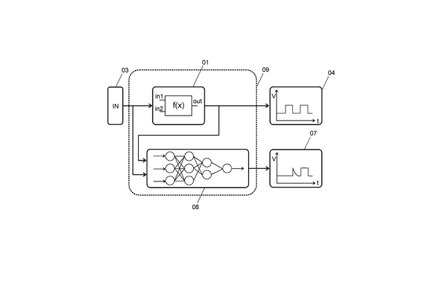
Behavioral models are important tools for electronic system-level design and verification due to their simplicity and fast computing time. However, this simplicity is a double-edged sword as it introduces model errors that are hard to keep track of. In this paper, we present an approach to estimate the model error of behavioral models by utilizing an artificial neural network. This can be integrated into system-level simulations and provides online, reliable information on the validity of the model. Knowing the model error allows to evaluate trade-offs by tolerating errors where possible and ensuring precision where needed. Considering computing time, the proposed approach is low cost and aides the designer to balance speed and precision in the behavioral modeling of complex circuits. To demonstrate the capabilities of this approach, we showcase the performance in a case study.
Spotting the gap in the design flow for superconducting electronic devices
Frank Feldhoff (1), Georg Glaeser (1,2) and Hannes Toepfer (1,2)
(1) Technische Universität Ilmenau, Germany, (2) IMMS Institut für Mikroelektronik- und Mechatronik-Systeme gemeinnützige GmbH (IMMS GmbH), Germany
Quantum technologies have matured in a way that real applications are considered to be viable. The new quality emerges from the use of explicit quantum phenomena in single objects as qubits for computation, or photons for sensing and communication. However, to make these features exploitable, suitable microelectronic components for controlling and read- out of the quantum states have to be available. For this, superconductive solid-state electronic circuits are considered to be promising candidates. First demonstrations for suitability are known. In order to provide scaling towards large-scale integrated structures, appropriate design methods and capabilities have to be developed. We provide an assessment of the current state of design automation for such superconducting digital electronic structures and survey existing approaches and tools.
Teaching the MOSFET: A Circuit Designer’s View
Ralf Sommer (1,2) and Carsten Gatermann (1)
(1) Technische Universität Ilmenau, Germany, (2) IMMS Institut für Mikroelektronik- und Mechatronik-Systeme gemeinnützige GmbH (IMMS GmbH), Germany
Metal Oxide Semiconductor Field Effect Transistors (MOSFETs) are the most common components within integrated circuits. That is why they are commonly taught in the courses of study for electrical engineers. Despite hundreds of papers and books on MOSFETs the intuitive explanation of its behavior rises questions of the students especially for the explanation of saturation behavior. Why is the current limited by the charge carriers that are in the semiconductor substrate and form the inversion layer? There is an almost infinite reservoir available from the battery and the terminals, isn't there? Why do the sets of characteristic curves not continue to follow the parabola instead of remaining constant from the peak point (transition from linear to saturation region)? The paper shows both the consistent and causal derivation of the Level 1 MOSFET behavior from a few equations and the illustrative explanations for students to understand this behavior. Finally, an outlook is given on today’s MOSFET models and the difficulties in interpreting especially their AC parameters.
Related content
Project
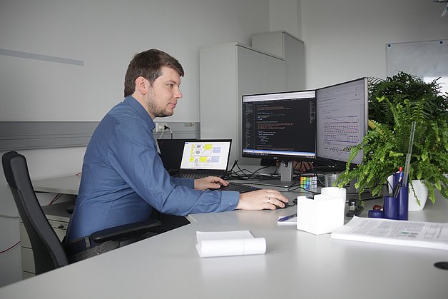
KI-EDA
IMMS developed smart models and tes methods for the design of sensor and control chips for I4.0 applications
Press release,
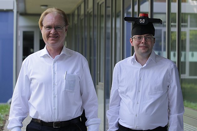
Reliable and faster chip designs through invasive and parametric simulation methods
Dissertation on new methods for automation in integrated circuit design
Press release,
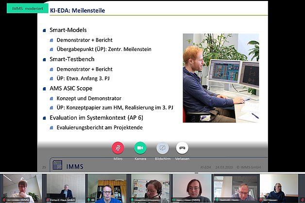
KI zum Entwurf von Antriebssteuerchips als Schlüsselprodukte für die Industrie 4.0
Virtuelles Kick-off-Meeting zum Projektstart von KI-EDA
This might also be interesting for you
Contact
Contact
Dipl.-Hdl. Dipl.-Des. Beate Hövelmans
Head of Corporate Communications
beate.hoevelmans(at)imms.de+49 (0) 3677 874 93 13
Beate Hövelmans is responsible for the text and image editorial work on this website, for the social media presence of IMMS on LinkedIn and YouTube, the annual reports, for press and media relations with regional and specialist media and other communication formats. She provides texts, photographs and video material for your reporting on IMMS, arranges contacts for interviews and is the contact person for events.


